Hall Effect Measurements
Before the discovery of quantum mechanics only the resistance R and conductance G considered as measurable physical quantities. Quantum mechanics deals with complex electrical transport measurement. i.e. density n and mobility µ.
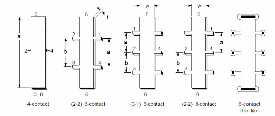
A Hall Effect measurement utilizes two sample geometries:
- Long and narrow hall bar
- Van der Pauw geometries.
In both, a Hall voltage is created perpendicular to a current and an applied magnetic flux (Akeyoshi, Matsuzaki, Itoh, Waho, Osaka, & Yamamoto, 1999).
Hall Bar
Examples of some of the Hall bar geometries are given below.
Hall Effect and properties of semiconductor
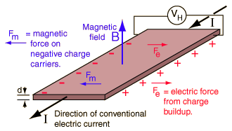
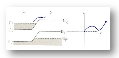
Semiconductor properties can be determined by the Hall Effect. For this purpose a magenetinc field is induced in the semiconductor which “is perpendicular in the current flow” direction (Bohm, 1967, pp. 32).
The Hall voltage that results is often perpendicular to the current and the magnetic field (Chua, 1999).
Hall voltage Origin:
The origin of the hall voltage is from a semiconductor bar which is a p-type. While both of “the applied electric field and the current are in the positive x-direction, the applied magnetic field is in the positive z-direction, and the y-component of the force” is shown by (Yong, 2004, pp.56).
![]()
What this equation explains is that all carriers which are travelling within the sample are subjected to a force that will move them to one side of sample (Chung, Yu, Jin, Park, Berger, & Thompson, 2006). Therefore, holes will tend to go towards the negative y direction (Day, 1990).
Right side of bar accumulates the large number of holes hence have a positive charge. An “internal electric field is created in the +y-direction. As the applied electric field is in the +x-direction, the force due to the internal electric field opposes the Lorentz force” (Chua, 1999).
For continuous current flow through the sample, balance of forces must exist:
![]()
As shown by the formula above, a net force does not apply on the carriers when they are moving towards the y-direction.
The internal field can be detected if the voltage created is measured as shown:
![]()
Where w is the width of the sample.
The “Drift velocity refers to the movement of carriers which are subjected to an electric force” (Figueiredo, 2008). The hole current in the sample can thus be expressed as follows:
Ip = q x p Vd x A
Where “+q is the hole charge, p is the hole density, vd is the drift velocity, and A is the cross sectional area” (Frensley, 1990, pp.78).
In order to convert this finding to an equation for the “current density vector, where the magnitude J = I/A and the direction is parallel to the drift velocity” gives the following (Witt, 2010, pp.12).
![]()
The drift velocity is associated an electric field that drives it through the proportionality constant that is termed mobility. Where:
![]()
If this relationship is applied in the equation for the filed Ey, the following is established:
![]()
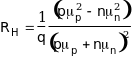
Where “RH =1/qp is called the Hall coefficient” (Akeyoshi, Matsuzaki, Itoh, Waho, Osaka, & Yamamoto, 1999, pp.24).
RH = –1/qn for n-doped samples.
In the presence of both holes and electrons, the Hall Effect will be shown by the following equation for small fields:
The Hall Coefficient measurements provide the following information about the solid:
- The sign (electrons and holes) of charge carriers.
- The type of material.
- The carrier concentration can be measured.
- The mobility of charge carrier.
- It can be used to determine the given material is insulator or semiconductor.
Background on RTD’s
In1958, L. Esaki was working on his PhD dissertation, he was studying heavily doped germanium p-n junction. He discovered an abnormal I-V characteristic in the forward direction; it was explained by the quantum tunnelling theory (Gennser, 1990). This was later on justified when it came to agreement with the experimental results. Afterwards researchers demonstrated this on other semiconductor materials, such GaAs.
”Resonant Tunneling Diode (RTD) is considered among the fastest devices because tunneling is very fast and is not transit-time limited” as in CMOS technology, etc (Bohm, 1967, pp.37). RTDs provide a low leakage current if a reverse bias is utilized. Large dynamic range within a small input voltage range However, the output current and power of RTDs is very limited compared to Complementary Metal Oxide Semiconductor (CMOS) (Haddad, 1998). RTDs can operate at frequencies up to several terahertz’s (THz), much higher than those corresponding to Esaki’s tunnel diodes which just reach about 100 GHz, with response time under
![]()
s. Small values of the negative differential resistance, i.e. an abrupt fall after the maximum of the I–V curve resulting in high cut-off frequencies of operation. In fact, RTDs are the only purely electronic devices that can operate up to frequencies close to 1 THz, the highest of any electron transit time device. Because of the RTDs ability to reach high switching speeds RTD is implemented in several applications. Such as imaging systems (Tsu, 1973).
Shortly after the Molecular beam epitaxy was used in research in the field of semiconductor crystal growth, the idea of resonant tunnelling in semiconductors was imposed, by Tsu and Esaki in 1973.
Transmission and reflection of electron waves through the double barrier structure are the tunnelling properties. Schrödinger equation can be used to solve this.
Need for RTD
Today’ s modern era of information technology is due to high speed compact and low cost the electronic representation and processing of information. For continuation growth of this, it demands further reduction of chip size. Chip size has been following the Moore’s law for last three decades and it seems continue to apply for some time in future. the miniaturizing of conventional transistors and integrated circuits will ultimately be reached. While the miniaturization of conventional transistors posses a special fast evolution, revolutionary device concepts have been vigorously sought, mainly in both related areas known as nanoelectronics, and single electronics. Many Variations of RTDs, became a the focus of research focus in nanoelectronics, because of its characterises as a major nanoelectronic device for the analogue, and digital applications (Tsai, 1994).
Why RTD
Because of the simple structure, and the relatively easy to fabricate, the very high speeds, and the versatility on the circuit function, RTDs have made to be research topics in nanoelectronics field.
Structure of the RTD
A resonant tunnelling diode (RTD) fabricated here consists of GaAs as the conducting layers, and AlAs as the insulator layer. Both insulating layers are positioned in the centre on the, sandwiched by the conducting layers. All of the motioned above layers are undoped, and the quantum confiment effect will happen between the GaAs layers and the AlAs, when bias is applied.
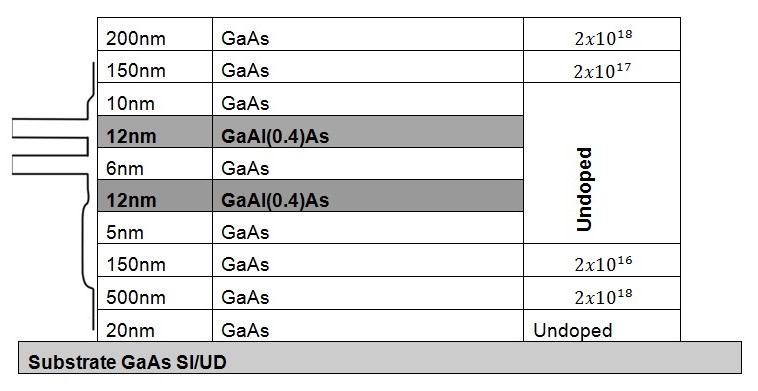
The multilayer structures shown in the above figure, were been deposited by the use of a molecular beam epitaxy in ultrahigh vacuum, where the thickness was precisely monitored and the composition achieved by the use of mass spectrometry in arrangement with a process control computer. This result is an extremely smooth unique film layers, as evaluated by both electron diffraction measurements and transmission electron microscopy. 8. 9 This is undoubtedly the most important requirement for the observation of resonant tunneling (Hollander, Manti, Zozoulenko, & Berggren, 2001).
RTD Performance with temperature
Temperature dependant is one of the most important features that any new technology must adopt. This is what distinguishable when it comes to RTD devices.
Several journals and papers showed that the peak value ration (PVR) regions of the RTD produce peaks at lower temperatures, this is because as the thermal energy increases, the electrons in the increase in distribution. When the electrons in conduction band align themselves with the holes in the valence band the resonant tunnelling occurs. If the thermal energy of the excited electrons is high due to applying bias on, this will result in a broader and higher peak. However, when the bias is further increased, this leads to much more excitement of the electrons due their high thermal energy, resulting in electrons going over the barrier (Sudirgo, et al., 2006).
Applications of RTDs
The functional applications of RTDs are highly promising, since RTDs can be embedded in conventional devices and bipolar transistors. The application include, static random access memories (SRAM), pulse generators, multi valued memory, multi valued and self-latching logic
Quantum Tunnelling
Quantum effect plays a significant role, when the size of a system is comparable to the electron wavelength. This occurs when transistors are miniaturised and their characteristic dimensions reach the nanometre range, this leads to possible novel devices and possibly a new phenomenon based on quantum tunnelling mechanisms. It is extremely important that the new devices are designed and fabricated in the nanometre precision and size, in order for nanoelectronics to become a reality, designing at nanoscale level requires a lot of precision and skills (Day, 1990).
This phenomenon is not directly perceived. Therefore, it’s “understanding is dependent on the understanding in the macroscopic area, which classical mechanics can adequately explain” (Witt, 2010, pp. 4). Quantum tunneling is the basis of the fundamental theory behind the operation of RTD, this study is based on the Heisenberg uncertainty principle, in which the electron able to tunnel through a barrier, which is not a possible case in classical mechanics, only in quantum mechanics this is phenomena can be explained. In order to elaborate on how the electron penetrates the barrier, the use of the Schrödinger equation is used. Three regions the electron travel in, wavefuctions for those regions are:
![]()
![]()
![]()
Where:
![]()
![]()
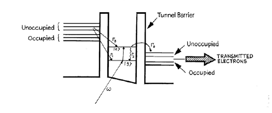
The electrons are free to move without any potential energy in the 1st and 3rd region, whilst in the 2nd region as the particle approaches the barrier, the process is known as the free particle wave function. The negative sign in the waves is to note that it is travelling in opposite directions.
The ability of electron tunneling to become confined in a quantum well is a fundamental aspect that any resonant tunneling diode must possess (Thomas, 2008).
The total energy possessed by the electrons Ek may be determined by applying the following equation:
![]()
Where m* is the electron mass, (kx, ky) are the lateral motion of the electron.
RTD Mechanism
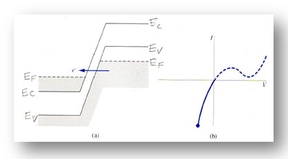
After talking about the process quantum tunnelling, it is a easier to understand how the RTD works. When the energy level outside the well is aligned with the energy level in well, the conduction band becomes aligned with the valence band and current will flow.
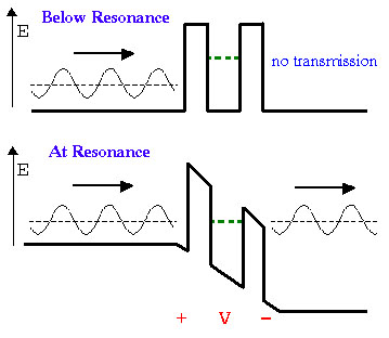
When the device is on resonance, a peak occurs in the I-V curve, further increasing of the bias will lead to the energy level falling out of alignment and transmission will terminate.
The wave number qR is relevant to the energy of the resonant state, which can be calculated from:
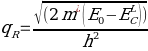
Where E0 resonance state energy in the quantum well, and ELC is the conduction band energy in the emitter (Slight, 2007).
As long as the resonance is stable throughout the transmission of the applied bias, the tunnelling current can be expressed like this:
![]()
Where:
![]() is the local Fermi energy, which is
is the local Fermi energy, which is ![]()
The relationship between ![]() and the applied bias is proportional, while J increases until the
and the applied bias is proportional, while J increases until the ![]()
falls below the conduction band edge.
Operation of the device
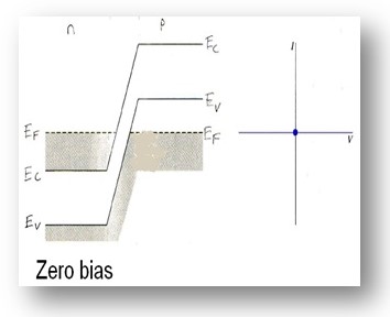
When applying no bias on the system, there is no tunnelling occurring
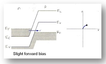
As the bias is applied the “electrons in conduction band are energetically aligned to the holes in the valence band” (Figueiredo, 2008). Tunneling takes place leading to the production of a forward current.
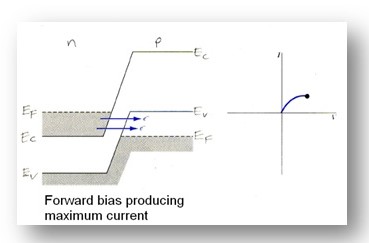
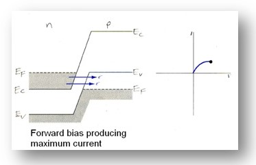
Further bias is increased to result into maximum current to be produced when all electrons in the conduction band align with all holes in the valence band (Chung, Yu, Jin, Park, Berger, & Thompson, 2006).
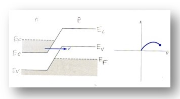
As bias still tends to further increase, the electrons in the conduction become less aligned with the holes in the valence bad, which results in less current being produced.
The alignment between electrons and hole is very poor, and the diffusion current dominates over tunnelling which results in termination of the current.
The bias increased significantly which allowed electrons to go over the barrier and allow the flow of current. Once this happens RTDs tend to look like a normal tunnelling diode in reverse bias.
Negative Differential Resistance (NDR)
NDR is “inversely proportional to the peak current” (Romeira, 2008). In order to attain high speeds a huge tunneling current is necessary, since the switching speed of a tunnel diode is depended on the current available for charging the junction capacitance and the average RC product (Gennser, 1990).
Electrons in heterojunctions and in quantum wells can respond with very high mobility to applied electric fields parallel to the interfaces. Under certain circumstances, electrons can tunnel through these potential barriers, constituting the so-called perpendicular transport. Negative differential resistance zones are visible in Tunnelling currents through heterostructures, this happens when the bias is significantly increased which results in a decrease of flow of current.
The operation of the devices fabricated based of the NDR quantum well was called Resonant Tuenneling effect (RTE) which took place when a current travelled through a structure created by a quantum well in between two thin barriers. The I–V characteristics of RTE devices were somewhat similar to that of Esaki’s tunnel diode.
Many researchers believe that RTD’s may be the future of device in the field of quantum confined heterostructure. The transition from research into practical application happened by progressing in the epitaxial growth, which has improved the peak to valley ratio (PVR) current ratio at room temperature beyond that what is required for many circuit applications that are characterized by the current peak to valley ratio as below (Coehoom & Boerner, 2008).
![]()
To achieve maximize dynamic range, high PVR is desired. And to obtain maximum output power from RTD, high current density is required. Decrease the thickness of the quantum well barrier. Increase emitter doping level. However, PVR will be decreased and leakage will increase
Commercial resonant tunnelling diodes (RTDs) used in microwave applications are based on this effect.
If RTDs are simulated by a negative resistance in parallel with a diode capacitance.
C and a series resistance RS, as is the case of normal diodes, it is relatively easy to demonstrate that the maximum operation frequency increases as C decreases. The resonant tunnel diode is fabricated from relatively low-doped semiconductors, which results in wide depletion regions between the barriers and the collector region, and accordingly, small equivalent capacity (Kwok, 2002).
Wafer Cleaning
To ensure that the sample is as clean as possible and free of contamination and foreign particles, different techniques are used for different scenarios, this project employed the techniques discussed below.
Particles Elimination
Insoluble particles are one of the common problems when it comes to cleaning a sample. To resolve the issue of removing particulates from the wafer, Ultrasonic scrubbing “Agitation” is used (Chua, 1999, pp. 55).
Ultrasonic scrubbing consists of “immersing the wafer in Acetone liquid and placing it in the agitator” (Witt, 2010, pp.13). The sonic agitation results into the formation and collapsing of microscopic cavities to, resulting into shock waves that loosen and displace particles (Mark, 1989). The negative side of ultrasonic scrubbing is that it might damage the sample by breaking it if the power was high. If contaminates still appeared on the sample, a use of a cotton swipe is used by dipped it in Acetone and swiping it across the surface of the wafer to remove any particles which were not removed from the agitation.
Photoresist Stripping
Photoresist stripping comes at a later stage in process of fabrication, and is the removal of unwanted photoresist layers from the wafer (Kosik, 2011). It aims to eliminate the photoresist material from the sample while preventing chemical attack to the surface materials utilized.
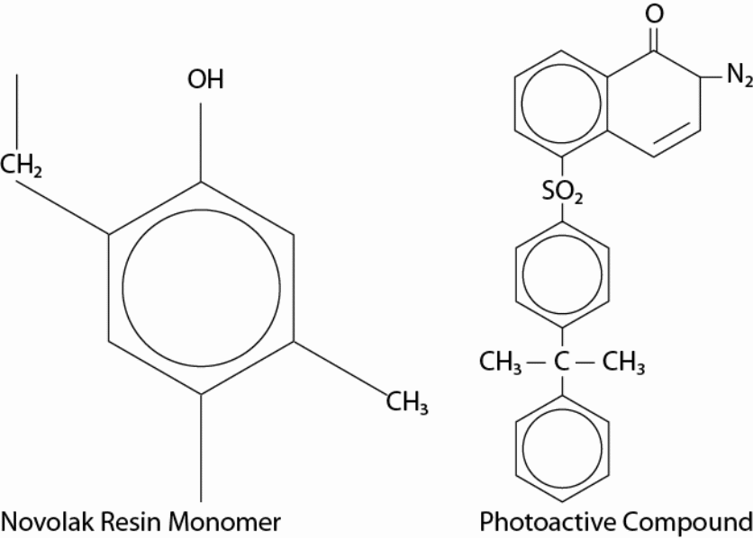
Lithography is the “process of defining the regions or patterns on the wafer where material is to be deposited or removed, or where dopants are to be introduced” (Madhukar, 1997, pp.98). A crucial part of lithography is the application of the photoresist, which refers to the “process of covering regions that either need to be consequently removed or retained with a light sensitive film called photoresist” (Frensley, 1990). The procedure by which materials are eliminated following photolithographic process is referred to as etching (Frensley, 1990).
Typical “resists consist of three components: the resin, which serves as the binder of the film,a photoactive compound, and the solvent” which controls the physical properties of resist (Yong, 2004, pp. 35).
Photoresist
The photoresist coating process is done by dispersing a small amount of photoresist was used on this wafer, it is a positive resist, the resist was dispersed on the centre of the sample, the quantity of the photoresist was dependant on the size of the sample (Logansen, 1964). The spinner was set to spin at 5000rpm for 45sec; while the sample is being spun the excess photoresist was being scrubbed off in the form of a spiral. This process gave a photoresist measured thickness of ~ 1.2µm.

Softbake
Here the sample was placed on top of a hot plate, at 115˚C for 60sec, this was used in order to reduce the residual solvent level in the photoresist, and anneals out residual stresses in the sample, coated photoresist improves adhesion, and it helps reduces the residual solvent levels which improves the difference in developing the rates between the exposed and unexposed portions of the photoresist. The hot plate has few advantages over the oven baking which can be used as well, such as, it is usually faster, more controllable, and does not trap solvent.
Exposure
When exposing a photoresist film to UV light, it becomes less acidic, and therefore it is vital to make sure that the correct regions are exposed. It is also important to expose the sample with the correct time, and make sure it is not over exposed nor under exposed. If it is under exposed, the photoresist will not be sufficiently acidic, and region of resist will remain after development. As well, there are also problems with over exposure, where the diffraction can make the protected areas exposed. These effects are present at all exposures, but during short exposure, the parasitic effect is very small.
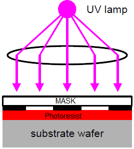
There are three methods used for exposure: Contact aligner, proximity aligner, projection aligner. This project employed the use of the contact aligner method, where the mask and substrate came in contact with each other. The contact aligner method has the advantage of transferring the smallest features from the mask to the substrate successfully. The UV source in the mask aligner used in this project has an intensity of 0.365µm.
Development
Is achieved in order to leave the resist pattern which was blocked from the UV light through the mask on the, which is going to protect the patterned areas from chemical attack during subsequent etching, and lift-off (Tsai, 1994). The development process “involves chemical reactions where unprotected parts of the resist get dissolved in the developer” (Haddad, 1998).
Development is performed by immersion and stirring sample in (MF-319) developing solution, as soon as the development process finish, the sample is taken out the beaker and blow dried using N2 gas to ensure that the development process does not carry on.
Etching
Is the process of “carving regions of the underlying material that are no longer protected by photoresist after development” (Tsu, 1973, pp. 35). Etch rate refers to the rate at which the etching course takes place. The “etching process is said to be isotropic if it proceeds in all directions at the same rate” (Day, 1990). If it proceeds in only one direction, then it is completely anisotropic (Tsu, 1973).
Two types of etchant are usually identified as follows: Dry Etchant and Wet Etchant. This project implied the use of the wet etching method. Wet etching, “or etching with the use of chemicals, is generally isotropic, while dry etching processes that employ reactive plasmas are generally anisotropic” (Romeira, 2008, pp. 56). A wet etch knows as “piranha etch” was used in order to obtain anisotropic etching of the sample. It is done by preparing a solution of H2O:H2O2:H2SO4 with concentrations of 40:8:1. Etch rate is temperature dependent. This has an etching rate of 1.5µm/min and a temperature of 80˚C. However, when allowed to stable and cool down to room temperature the etch rate reduces to ~ 0.9µm/min.
Metal Deposition “Metallization”
It “refers to the metal layers that electrically interconnect the various device structures fabricated on the silicon substrate” (Witt, 2010, pp. 12). The Laying of the metal contacts is vital because it is how the device is going to be connected to the package and would define the characterizations of the device. Edwards thermal evaporator was used in order to achieve deposition of the metal, two evaporators were used the semi-auto Edwards, which has the a mechanical lever to choose between metals wanted to deposit, and has a turbo pump, leading to a faster pumping down which was approximately 30minutes, and it was used to deposit the Ti and Au. While the Edwards manual evaporator can only hold one metal at once, and has a rotary and a diffusion pump, it was much slower to pump down, and took approximately 2 hours at least before starting to evaporate; it was used to deposit AuGeNi. Both evaporators took approximately the same time to evaporate the metal. It was mainly a matter of the rate per second when it came to the evaporation speed and in both evaporators the rate was maintained at 0.1nm/sec (Chung, Yu, Jin, Park, Berger, & Thompson, 2006). The evaporation starts when a current is applied across a tungsten boat which contains the metal wanted to deposit, then boat heats up heating the metal containing it, the metal with the lowest metal point will evaporate first. The boat can withstand temperatures up to 3659K, which is the melting pint for the boat. Boats can break duo to excessive heat though, and then there is a need to replace it and “flash” the new boat by suppressing it high currents (Thomas, 2008).
Thermal Annealing
It is a process where the sample is heated to very high temperatures, for short periods of time (seconds). Temperatures need to be heated up and cooled down slowly, thus not to break or damage the sample due to thermal shock. This rapid heating is caused by a set of halogen lamps. Thermal annealing allows the diffusion of the metals into the wafer, resulting in better ohmic contacts (Akeyoshi, Matsuzaki, Itoh, Waho, Osaka, & Yamamoto, 1999).
Scriber
This step is used to initiate a scribe line through the pattern needed to be cut, this is to ease the actual cutting of the sample and make it as precise as possible. The method used is the scribe and break die separation (Gennser, 1990). Scribe and break “separation of wafers is achieved by introducing the wafer to stress and then fracturing the wafer along the stress line” (Madhukar, 1997, pp.13). A scribe line must be created in the wafer surface where the sample wanted to broken. The wafer will break by applying force on it, along the created line because this line creates a stress factor. The depth of the scribe is not as significant to help with the break as much as the sharpness of the bottom of the scribe, due the larger effect which that sharpness has on creating the stress factor. Since diamond is the sharpest metal known it can achieve a high stress concentration. As for breaking the sample into pieces, a method known as “static breaking” was used, which require a bending force by hand to be applied on the sample at a force that will make the wafer crack along the scribe made by the scriber (Thomas, 2008, pp. 30).
Packaging
After the wafer is cut into smaller pieces, they are installed in a leadless chip carrier also known as “package”, they are installed by high precision by applying a small droplet of super glue into the middle of the package and resting the freshly cut piece on top of the glue, making sure that the sample is leveled, a verification is made my imaging the package under a microscope with low magnification and making sure that the entire sample is in focus and can be imaged without adjust the focus for different parts of the sample (Chung, Yu, Jin, Park, Berger, & Thompson, 2006).
Wire Bonding
Is a process that involves the connection between the device that is fabricated and the package via a gold wire (Day, 1990). This is done by a combination of pressure and temperature making it possible to weld the gold wire, leading to the ability to test the electrical characterizations of the device. Two techniques are implied in the University of Leeds to wire bond the sample to the connections on the package.
The Ball Bonder and the Wedge Bonder
The wedge bonder uses ultrasonic vibrations to bond the wire into the package and the sample, and is preferred for highly sensitive electrical devices. However, with the Ball Bonder, a small electric current is a applied in order to bond the gold wire to the package and the device, forms a bond in the shape of a ball (Yong, 2004). The Ball bonder was used during the fabrication of this device.
References
Akeyoshi, T., Matsuzaki, H., Itoh, T., Waho, T., Osaka, J., & Yamamoto, M. (1999). Applications of Resonant-Tunneling Diodes to High-Speed Digital ICs. Indium Phosphide and Related Materials , 11:405-410.
Bohm, D. (1967). Quantum Theory. New york : Prentice-Hall.
Chua, S. S. (1999). Shot noise characteristics of a resonant tunneling diode. J. Phys. D Appl , 27: 137-141.
Chung, S. Y., Yu, R., Jin, N., Park, S., Berger, P., & Thompson, P. (2006). Si/SiGe
Resonant Interband Tunnel Diode with fr0 20.2 GHz and Peak Current Density 218 kA/cm2 for K-band Mixed-Signal Applications. IEEE Electron Device Letters , 27:364.
Coehoom, R., & Boerner, H. (2008). White Organic Light -emitting Diodes. New York: Wiley.
Day, D. J. (1990). Double quantum well resonant tunneling diodes. Applied Physics Letters , 57:1260.
Figueiredo, J. M. (2008). Self-oscillation and period adding from resonant tunnelling diode–laser diode circuit. Electronics Letters , 44:876.
Frensley, W. R. (1990). Boundary Conditions for open Quantum Systems Driven Far From Equilibrium. Rev.Mod Phys , 62:745-791.
Gennser, U. (1990). Resonant tunneling of holes through silicon barriers. ournal of Vacuum Science & Technology B: Microelectronics and Nanometer Structures , 8:210.
Haddad, S. G. (1998). Resonant Tunneling Diodes: Models and Properties. Proceedings of the IEEE , 86:641-660.
Hollander, B., Manti, S., Zozoulenko, V., & Berggren, K. (2001). High Performance Si/Si1-xGex Resonant Tunneling Diodes”. IEEE Electron Device Letters, 22:182.
Kosik, R. (2011). Resonant Tunneling Diode Structure. Web.
Kwok, K. (2002). Complete Guide to Semiconductor Devices. New york : Wiley.
Ling, J. (2010). Resonant Tunneling Diodes: Theory of Operation and Applications. New york: University of Rochester.
Logansen, L. V. (1964). The possibility of resonance transmission of electrons in crystals through a system of barrier. Soviet Physics , 18:146.
Madhukar, R. (1997). Schottky-collector Resonant Tunnel Diodes for Sub-Millimeter-Wave Applications: Web.
Mark, S. (1989). Resonant interband tunnel diodes. Applied Physics Letters , 54:546.
Romeira, B. (2008). Synchronisation and chaos in a laser diode driven by a resonant tunnelling diode. ET Optoelectronics , 2:211.
Slight, T. J. (2007). Investigation Into the Integration of a Resonant Tunnelling Diode and an Optical Communications Laser: Model and Experiment. IEEE Journal of Quantum Electronics , 43:580.
Sollner, T. C. (1983). Resonant tunneling through quantum wells at frequencies up to 2.5 THz. Applied Physics Letters , 43:588.
Sudirgo, S., Pawlik, D., Kurinec, S., Thompson, P., Daulton, J., Park, S., et al. (2006).
NMOS/SiGe Resonant Interband Tunneling Diode Static Random Access Memory, 64th Device Research Conference Conference Digest. University Park: The Pennsylvania State University.
Thomas, S. (2008). A LiÉnard Oscillator Resonant Tunnelling Diode-Laser Diode Hybrid Integrated Circuit: Model and Experiment. IEEE Journal of Quantum Electronics , 44:1158.
Tsai, H. H. (1994). P-N double quantum well resonant interband tunneling diode with peak-to-valley current ratio of 144 at room temperature. IEEE Electron Device Letters , 15:357.
Tsu, R. (1973). Tunneling in a finite superlattice. Applied Physics Letters , 22:562.
Witt, G. (2010). Resonant Tunneling Diode Research. Web.
Yong, C. S. (2004). Three-terminal Si-based negative differential resistance circuit element with adjustable peak-to-valley current ratios using a monolithic vertical integration. Applied Physics Letters , 84:2688.